- Joined
- Jun 7, 2012
- Messages
- 15,469
- Reaction score
- 7,848
- Location
- Central Florida
- Website
- www.flickr.com
- Can others edit my Photos
- Photos NOT OK to edit
The raw files from my 16mp fuji were bigger than the raw files from my 24mp d7100
Follow along with the video below to see how to install our site as a web app on your home screen.

Note: This feature currently requires accessing the site using the built-in Safari browser.
pixmedic said:The raw files from my 16mp fuji were bigger than the raw files from my 24mp d7100
long time lurker, first time poster, can't let this one go.
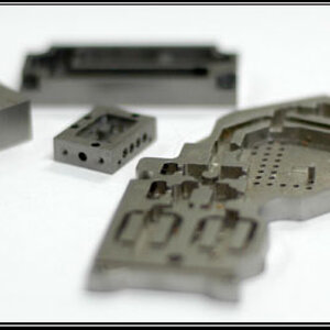
original post is total BS. virtually all parts on that PCB are BGAs, which can be reworked but v. challenging and, this is important the one tool you do not use is a soldering iron.
what ever LOL how ever there is no way to remove and replace the chip with out the soldering..
Donny
well i used an iron lolsolder yes soldering iron no
see, e.g., BGA rework
note list of tools. no soldering iron. you simply do not use this tool anywhere in a BGA rework. sorry. you use heat guns or an oven. an iron creates spot heat which will destroy a BGA, you need uniform heat to even remove any surface mount technology. surely you know this since you worked at flex.
First off it wasn't a chip like that... i wouldn't spend that amount of time..
a chip like that...
The chip your talking about is a processor chip, the memory chip is nothing like that what so ever..whut?
that's what all the chips on the D810 main board are like. go look at any teardown web site. for any camera, not just the D810. they're all
a chip like that...
so. whut. what you're describing is literally impossible. not challenging, not difficult, not unlikely, literally impossible. which is why i'm posting in the first place. anyways i think we're done here.
whut?
that's what all the chips on the D810 main board are like. go look at any teardown web site. for any camera, not just the D810. they're all
a chip like that...
so. whut. what you're describing is literally impossible. not challenging, not difficult, not unlikely, literally impossible. which is why i'm posting in the first place. anyways i think we're done here.
The memory chips on the board are not pins that go strain down they are pins that come out the side then down, they are not what you are describing...you don't give up easy do ya? all the chips on a camera mainboard are BGAs. you must have the old memory buffer chip out of the D810 lying around handy, right? post us a picture of it. just grab your phone, take you 30 seconds.
i didn't say they was mine lol i said the boards are not BGA, i'm not tearing down my nikon to show you my boards.stolen pics of canon guts.
Camera and Photography forum | Cameralabs • View topic - Weathersealing in practice - your experiences please!
and
Ben trong may anh Canon EOS 5Ds co gi
for shame.


![[No title]](/data/xfmg/thumbnail/32/32929-22e23acc63d6ecb25e5ee941be87121f.jpg?1619735758)